Showing posts with label project. Show all posts

5/08/2013

50 watt Power Amp OTL by LM3900, 2N3055


This be power amp OTL 50Watt use IC LM3900 and 2N3055 x 3pcs transistors to pillar equipment. Follow very circuit keeps to are Class ab then have a voice good loud. When , be amp OTL you then are certain that build easy use power supply the group is one 70V sizes by must use Current low 2Amp go up. Then have a voice good another thing you will like that amplifier. This durability do not make a loudspeaker a lose easy.


LM3914          IRF3205           PT4115          2N2222A            NRF24L01


Digital voltmeter using ICL7107

The circuit given here is of a very useful and accurate digital voltmeter with LED display using the ICL7107 from Intersil. The ICL7107 is a high performance, low power, 3.5 digit analog to digital converter. The IC includes internal circuitry for seven segment decoders, display drivers, reference voltage source and a clock. The power dissipation is less than 10mW and the display stability is very high.


The working of this electronic circuit is very simple. The voltage to be measured is converted into a digital equivalent by the ADC inside the IC and then this digital equivalent is decoded to the seven segment format and then displayed. The ADC used in ICL7107 is dual slope type ADC. The process taking place inside our ADC can be stated as follows. For a fixed period of time the voltage to be measured is integrated to obtain a ramp at the output of the integrator. Then a known reference voltage of opposite polarity is applied to the input of the integrator and allowed to ramp until the output of integrator becomes zero. The time taken for the negative slope to reach zero is measured in terms of the IC’s clock cycle and it will be proportional to the voltage under measurement. In simple words, the input voltage is compared to an internal reference voltage and the result is converted in a digital format.

The resistor R2 and C1 are used to set the frequency of IC’s internal clock. Capacitor C2 neutralizes the fluctuations in the internal reference voltage and increases the stability of the display.R4 controls the range of the voltmeter. Right most three displays are connected so that they can display all digits. The left most display is so connected that it can display only “1” and “-“.The pin5(representing the dot) is connected to ground only for the third display and its position needs to be changed when you change the range of the volt meter by altering R4. (R4=1.2K gives 0-20V range, R4=12K gives 0-200V range ).
Circuit diagram.

Notes.

    Assemble the circuit on a good quality PCB.
    The circuit can be powered from a +/_5V dual supply.
    For calibration, power up the circuit and short the input terminals. Then adjust R6 so that the display reads 0V.
    The ICL7107 is a CMOS device and it is very sensitive to static electricity. So avoid touching the IC pins with your bare hands.
    The seven segment displays must by common anode type.
    I assembled this circuit few years back and it is still working fine.


4/27/2013

LM393N integrated Circuits (ICs)

A TMOS power FET, Q1, and an LM393N comparator provide a high-efficiency rectifter circuit. When VA exceeds VB, U1's output becomes high and Q1 conducts. Conversely, when VB exceeds VA, the comparator output becomes low and Q1 does not conduct.

The forward drop is determined by Q1's on resistance and current I. The MTH40N05 has an on resistance of 0.028 Ω; for I = 10 A, the forward drop is less than 0.3 V. Typically, the best Schottky diodes do not even begin conducting below a few hundred mV.

4/26/2013

pulse signal interfaces EPC1PC8


The pulse signal examined is a driving signal of the power, used in the propulsion power to support, the drive current is usually several mA to several numerous mA, adopt the open-collector gate OC The form is exported, it is usually 12 – 30 V signal. For compatible many kinds of signal levels, and can isolate power type signal and ordinary base band level signal, realize better electromagnetic compatibility, this system adopts the photoelectric coupler as signal isolation and interface device of level switch.

TLP121 is the photoelectric coupler that Toshiba produced, isolates impedance as M grade, its drive current of forward direction IF Maximum 20 mA, rear end switch open and make time ‘s s grade, can respond to the request that the error in emasurement of this system pair is not greater than 1 ms. The input interface resistance is set as the adjustable resistance, can adapt to different input voltages.

The pulse signal interface circuit is shown as in Fig Straight line and loop of pulse signal are connected to the forward end 1, 3 pins of TLP121 in Fig of the photosensitive resister ,Rear end 4, 6 pins of TLP121 in Fig Adopt 5V power in the board to pull upward, sends and deals with FPGA to the interface after having a facelift through the Schmidt circuit 74HC14. When the pulse signal is effective, photosensitive resister forward end have electric current flow through, interface circuit export the intersection of high level and ” the 1 ” ; When pulse signal invalid, interface circuit export the intersection of low level and ” the 0 ” .

interface treatment FPGA

Because need to gauge pulse signals of No. 80, it is unable to meet concurrent processing’s demands to adopt the one-chip computer, so choose FPGA and finish the impulse sampling function. Interface deal with FPGA adopt the intersection of Altera and FLEX10K50 of Company, working primary frequency is 6 MHz, the storage chip adopts EPC1PC8.
Its main function has three parts: Frequency demultiplication timer, sampled data buffer, peripheral control logic. FPGA carries on the frequency demultiplication to the main clock, forms cycle as the clock signal of 1 ms. FPGA every ms finishes running side by side and gathers the pulse signals of No. 80 once, leaves the data in the register, send out the interrupt signal to the one-chip computer at the same time, notify the one-chip computer and initiate the data to move, and the time counter within the one-chip computer increases by oneself. The sampled data buffers the module and is used for latching the pulse signals of No. 80 to the internal register at the same time, the one-chip computers every ms all read once. Peripheral control logic is used in the decipher of every control signal of periphery of the one-chip computer, including control register, every chip control the signal interpretation, and the realization of other auxiliary functions.

4/25/2013

INA128, Adding -9V offset with reference pin BAV99


There is a bipolar (-10V/+10V) ADC on my circuit. And want to measure 0V to 5V signal with high empedance circuitry. To not loose ADC resolution I want to add a negative offset in INA128 circuit without using second amplifier. (0V to 5V  input;  -9V to 8.5V output) Theroticaly and experimentaly (using TINA-TI)  applying -9V to INA128 reference input solve my problem. Input and output voltage seems to be within specified limits but what about internal node voltages.

According to my calculation; when input is 5V and output is 8.5V,  A2 output node should be 11.25V.  But it seems difficult the reach this level with 12V supply. (Is it RRO)

Could you please clearify and make me sure for these ?

1.) Reference input is just intended for applying small offset nulling voltages or can I use it to apply higher offset ?

2. ) Using -9V offset is adequate for INA128 ? If yes how does it effect the CMRR ?

3.) Using 15V positive supply for INA128 allows me to apply -9V offset to reference pin if 12V supply is not enough?
a

( Diodes are BAV199 but not found in TINA-TI library so I used BAV99 instead. )

4/21/2013

Mono Power Amplifier A1015, BD140 ,TIP2955


Mono Power Amplifier - A1015, BD140 ,TIP2955 Circuit Diagram


Typically audio amplifier stereo amplifier to a two amplifier. And if a mono amplifier is a single speaker. However this circuit command be present extended to the mono two loudspeaker.But not a equivalence or else serialization access.This makes it needless impedance of the speaker has altered.But will remain to utilize the spokeswoman as a replacement for of the resistance - Collection Peter (RC) of the transistor.The circuit can be alive prolonged to 2 loudspeaker itself.

What time raising the power supply circuit and the audio to input. the audio sign coupling to through the C1 and R1 to increase with the Q1.Which Q1 serves like the Regional Pre amp amplifier to power up to a one point.already conveyance it to Q2.Which Q2 is connected to emitter follower circuit.be active as a driver amplifier intimate section from the pre amp section provides added power to drive the Q3 perform. and Q3 motivation provide while a Regional Power amp amplifier output to the spokeswoman.The opinion of the audio intimate through the VR1 and R2 to enter the pin B of Q2.To control the stability of working instead of well brought-up.This circuit is an output of 40 milliwatts watts of distortion of the gesture rate is by the side of 0.1 percent.And frequency response from 15 Hz - 200 kHz.

4/11/2013

CA3046 VCA


Using discrete transistors from a transistor array, this circuit avoids an OTA altogether. It uses one transistor as a Gilbert multiplier to predistort the signal, so that a larger signal can be fed into the circuit. The circuit is based on the one described in Modulus issue 5, that was provided by Chris Crosskey.
I have modfied it with a trimmer to adjust the DC offset and adjusted the input sensitivity and output gain to give some headroom and unity gain. This VCA has a linear response. A diode has been added on the control input, to block out negative voltages, which cause DC on the output. Because of the diode, the control caracreristics is unlinear below 1 volt.
The predistortion really works in this circuit. The distortion stays low up to a point where it suddenly increases dramatically. With the chosen resistor values, that point is well above normal signal levels.
Noise figures for this circuit is comparable to the SSM2024 and the LM13600 but signal bleedthrough is not as good. On the other hand, CV bleedthrough is lower than the LM13600, with proper trimming.


CA3046

4/10/2013

LM317T Variable Voltage Regulator


The LM317T is a adjustable 3 terminal positive voltage regulator capable of supplying in excess of 1.5 amps over an output range of 1.25 to 37 volts. The device also has built in current limiting and thermal shutdown which makes it essentially blow-out proof.

Output voltage is set by two resistors R1 and R2 connected as shown below. The voltage across R1 is a constant 1.25 volts and the adjustment terminal current is less than 100uA. The output voltage can be closely approximated from Vout=1.25 * (1+(R2/R1)) which ignores the adjustment terminal current but will be close if the current through R1 and R2 is many times greater. A minimum load of about 10mA is required, so the value for R1 can be selected to drop 1.25 volts at 10mA or 120 ohms. Something less than 120 ohms can be used to insure the minimum current is greater than 10mA. The example below shows a LM317 used as 13.6 volt regulator. The 988 ohm resistor for R2 can be obtained with a standard 910 and 75 ohm in series.

When power is shut off to the regulator the output voltage should fall faster than the input. In case it doesn't, a diode can be connected across the input/output terminals to protect the regulator from possible reverse voltages. A 1uF tantalum or 25uF electrolytic capacitor across the output improves transient response and a small 0.1uF tantalum capacitor is recommended across the input if the regulator is located an appreciable distance from the power supply filter. The power transformer should be large enough so that the regulator input voltage remains 3 volts above the output at full load, or 16.6 volts for a 13.6 volt output.

4/07/2013

FM Stereo decoder using TDA7388

A very simple with a compact design FM stereo decoder schematic circuit can be designed using the TDA7388 IC manufactured by ST Microelectronics .
The TDA7338 is a monolithic integrated stereo decoder with noise blanking for FM car radio applications.
With the used BICMOS technique, the 19KHz Notch Filter, the PLL Filter and Phase Filter is realized on the chip with a Switched Capacitor concept.
The TDA7338 stereo decoder contains all necessary functions for processing the MPX signal.
The only external component needed for the PLL is the ceramic resonator for the oscillator which runs at 456kHz.


The pilot detector output is designed as an open collector output, therefore an external pull up resistor is needed. To force the decoder to "MONO" Pin 19 has to be clamped to a voltage below 0.8V.
Selecting VCO-OFF (Pin 7 to GND) the VCO is switched off and the SB and HCC are disabled.
This TDA7338 receiver circuit needs to be powered by a 9 volts DC power supply .

3/28/2013

Big Motor Driver TLP250


I have posted a motor controller design that is supposed to be simple, robust, cost effective, and able to handle high currents.  Above is a schematic of the first part of the design.  I will post an updated version to include a PIC to accept commands from a PC, Microcontroller, etc. and provide the direction/PWM signals to the H-bridge.  I am still working on the PCB but here is what I have done so far for review/critism.  What is not shown in the schematic are the in-line fuses for protection.

For the PIC, I use MBasic and PicBasic Pro to write the code.  This should convert easly to the BS2 and PicAxe.


 I updated the schematic again.  As suggested I changed the MOSFET driver to a TLP250 and dropped the 1K resistor across the Gate to source.
Update the schematic to show that the logic grounds are isolated from the dirty motor grounds.


Finished the PCB design.  Once boards are complete will test and post schematic and board files once any kinks are worked out.


I got the prototype boards back from the manufacture two days after I sent them off.  As you'll see below, the quality is excellent.  Tonight I populated the board and checked out functionality with a multimeter prior to testing with a motor.  I managed to get everything put together right so on to the smoke check.  I hooked up a good size motor with a lot of torque and applied power.  The motor moved in both directions and the MOSFET did not even get warm.  This test was applying full power to the motor and not PWM.  Next, I'll write some code and test functionality with PWM hooked to my Oscope so I can check the signals and see how high I can take the frequency.  I'll get around to posting some video but, in the mean time, here are some pictures of one of the finished boards.


3/27/2013

Final Project - Ping Pong Shooter L7805CV


The Ping-Pong shooter, as its name, is able to shoot Ping-Pong balls, and the machine can simulate a real-world situation that if there is a player in front of it, it starts shooting; otherwise, it stops working

Criteria of Success
1. A machine that can shoot
2. Able to control the machine i.e. control weather the ping-pong ball will shoot or not
3. Able to control the system with a laser dependent switch


How it works:
The ping-pong shooter mainly contains three parts
1. A switch that is depends on a photoresistor and a light source(laser beam)
2. Two DC motors to shoot the balls
3. Stepping mother which acts likae a gate to control the flow of the ball


Main Component

    Photoresistor
    DC motors
    Stepping Motor (a8byj-48)
    Micro controller (89S51)
    Octal high voltage high current Darlington transistor arrays (ULN2803)
    Voltage regulator (L7805CV)


    A ULN2803 is an intergrated Circuit (IC) chip with a HIGH Voltage/High Current Darlington Transistor Array. It allows you to interface TTL signal with higher voltage/current loads
    The chip takes low level signals (operate at low voltages and low currents0 and acts as a relay of sorts itself, witching on or off a higher level signal on the opposite side.


    The 78xx family is commonly used in electronic circuits requiring a regulated power supply due to their ease-of-use and low cost
    I.E. 7805=5V   7812=12V
    Disadvantage: Input voltage always needs to be higher than the regulated voltage

Miscellaneous Component

    Resistor (10k ohm *2)
    Capacitor (33 pF*2,1000nF*1)
    Oscillator(12MHz*1)
    Wires
    PVC tube (2" Diameter)

3/26/2013

Box of MOSFET BS170


I was talking to a friend about distortion boxes and the Box of Rock came up. Which got me thinking, I’d never heard one before, and Z Vex always makes good stuff. I found a schematic in the usual place. It looked like a pretty easy build.


The Box is basically two pedals in series, a distortion followed by a booster. The Box has two foot switches, The first switch engages the distortion and the second engages the booster. The controls for the distortion are Gain, Tone and Volume. The booster adds a fourth knob, Gain/Boost.

The distortion section is made of three BS170 MOSFet stages. The first stage is a SHO followed by a Marshall style high pass filter made of a 470p cap and a 470K resistor in parallel. Then come two more BS170s configured gains of approximately 51 and 15.

Next is a BMP style tone stack followed by an extra low pass filter. The low pass filter is exactly the same as used in the BSIAB II. The BSIAB II also uses the same Marshall style, 470p and 470K, high pass filter between the first two stages.

The B of R includes an SHO booster on the output. I had one of these built already so i decided not to build the stock B of R and instead build just the distortion section. I figure I can place my SHO or any other booster after it for different sounds.


I also decided to change up the tone control for a little more variety and to make this into something a little different. I had heard a few good words about the James Tone control a.k.a. Baxandall tone stack. This is a two knob type with a Bass and Treble control. A good description of this tone stack can be found here. Here’s a shorter less technical description.


Here’s an image of the James/Blaxandall tone stack. RT and RB are the Treble and Bass control. I had run into this tone control before at Freestompboxes.org in a project by forum member Mictester. It was included as part of a project called Bigmuff Plus. This was sort of a BMP on steroids. My drawing includes values for the Orange Amp tone controls and the values used in the Big Muff Plus.

Note that the Blaxandall uses the Audio taper pots for the Bass and Treble controls. These are not required but, without them the usable adjust range is bunched up at one end of the pot rotation.


I drew everything in my notebook. At this point I had the following (note this omits the extra low pass filter and volume pot):


I built everything on a breadboard to test out the idea. I tested each stage as I built it. One thing that impressed was how bad the distorted sound was without a tone stack. I shouldn’t really say “bad” as the sound wasn’t terrible. Heck, it’s distortion right, so it might sound good to somebody. What is “bad” when it comes to distortion? The sound did lack the refinement and had some extra high end hash that wasn’t helping in my opinion. Through headphone the sound was unbearable. The headphone, I’m guessing, were reproducing more high end then would come out of a guitar speaker. After adding the tone control the sound was much smoother and had a lot to recommend it.

Later I added the extra low pass filter following the tone control. This really moved the sound into the Marshall territory. This kind of extra fixed filter stage added to the end made a noticeable difference in the sound. Seems like it might be a good addition to a lot of boxes.

Originally I had planned on using the Orange tone stack. Turns out I could only find a single A1M pot. Looking over Mictester’s take on the Blaxandall, he used different resistor and cap values alone with a A470K pot for the treble control. I did happen to have an A500K pot (with detents, it clicks at each of sixteen steps). So I Decided to go with those values. Some times you have to just work with what’s available.

I drilled a box fit all the parts and wired up the standard box connections. I drew up a perf board layout which placed all of the transistors in a row. I noticed at this point that the BS170 is DGS while the 2n7000 (another MOSFET) is SGD, seems like it would possible to swap these.


I’m not the greatest at making flowery descriptions, but here goes. The sound is tight and crunchy. You can dial in a surprising amount of low end with the bass control. The bass is tight and doesn’t get muddy. It’s got a sound you would associate with Marshall amps. I’d say it does AC/DC to Van Halen. It doesn’t quite get to metal.

The added low pass along with the higher impedance tone stack cut the output noticeably. The volume needs to about 3 o’clock for unity gain. Might be good to add another transistor on the end to boost the volume. Then again maybe tinkering with the volume pot might be enough.

3/21/2013

Ultimate jewel mod 4N25


My aim was to make a light up jewel (like everyone else) but this jewel had to be different. So basically I set about adding other features and the like to it.
This is what I've come up with and after you’ve read this you'll no doubt have a whole lot of similar, maybe even better ideas based on this design.

What I've ended up with is:
1. A jewel that’s glossy black when the console is off
2. Which glows blue when the console is on
3. Which glows red when there's harddrive activity

Most of these ideas are just transferred from a clear acrylic PC case mod that I did last year!


What you need:
car window tint
spray bottle
small squeegee
Wire - lots of thin gauge wire
4 x red LED’s
4 x blue LED’s
+ The resistors to go with them
For the blue/red LED’s we'll be using the 12volt power source
or if you can, try to get tri-colour LED's, they give you a better effect.
Lots of heatshrink - this is your safest bet as it makes the job incredibly easy and safe IMO
Hairdryer - to heat the heatshrink
Solder and soldering iron
Hot glue gun


Circuit
A piece of strip board
4N25 Opto-isolator
ULN2803 IC
1N4148 Diode
2 x 10K Resistor


3/20/2013

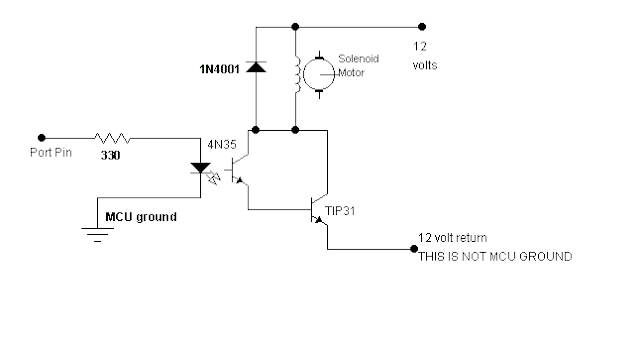
Solenoid and Sensor Control 4N35


To control the solenoid motors, we elected to use optoisolators. The control pins of the MCU were attached to the optoisolators which turns on and off the solenoid by controlling a TIP31 transistor. The TIP31 serves as an on/off switch for the solenoid. The optoisolators (4N35) were needed so that the MCU was completely isolated from the circuit. This protected the MCU because there were no physical connection between the MCU and the power supply. The 4N35 works by using a phototransistor that senses LEDS when the device is turned on.


The sensors were measured by a voltage division circuit coupled with an operational amplifier to achieve the desired results. The voltage outputted from the sensors was sent to the ADC of the MCU. The reference voltage of the MCU ADC was set to 5.0 volts which would correspond to the digital value 255 since only the top 8 bits of the ADC were used. We simply used this digital value to determine exactly how much juice we have dispensed.

3/19/2013

A Simple TX for Experimentation 2N7002 project


OK, so back to practical stuff on the bench. I breadboarded a simple push-pull power-oscillator using a pair of 2N7000 MOSFETs, operating in the HF region. (I've attached an LTSpice model if you want to tinker with it, I used a 2N7002 model and asymmetric bias resistors to keep spice happy, the real circuit uses 2N7000s and starts just fine with 4k7 bias resistors on both sides.)

The "180p" capacitor tunes the tapped coil to the frequency of operation, select or make it variable as desired. In one implementation I put 6v8 zener diodes on the MOSFET gates to protect them against over-voltage destruction, at low powers this is not strictly needed, but at higher powers you may need them. Similarly the pair of 33 pF feedback capacitors need to be selected with the frequency of operation in mind. The MOSFET drain breakdown voltage is also important if you are trying to scale up this circuit. While simple, other approaches are probably better for high powers, the MOSFETs are spending a lot of time in their transition regions, dissipating a lot of power. A purely switching class-E approach is obviously better, but suffers from sensitivity of tuning to load impedance in my brief experiments with it (using an IRF510 device). (I've attached another spice model attempting to show the class-E TX approach, I started with values derived using my class-E power amplifier design calculator, as shown it is not perfectly tuned. The practical circuit tunes up nicely and is quite efficient > 70%.) The breadboard TX in the video above is a class-C version with weak capacitive coupling to the tank to optimise its Q. Yet another approach is half or H-bridges, these show great promise, perhaps driving a magnetically coupled "link" winding rather than the tank directly, allowing the tank to float, and facilitating easy variation of coupling to it to optimise its Q... A subject for more detailed investigation at a later date perhaps.

3/18/2013

Driving Circuits from a CR2032 Lithium Coin Cell


Recently I have tested an complete over the top design which pushed the poor little CR2032 far beyond its limits. Time to grab a few facts from the datasheet for further reference.

To get a good example I found a quite elaborate CR2032 datasheet from Duracell. I think other batteries behave quite similar to this.

The general key fact of an CR2032 are obvious and quite easy to grab from the datasheet:

Voltage: 3V

Capacity: 240mAh (to 2.0V)

If you study the datasheet more closely you will see that the voltages drop sharply after it reaches 2.8V (after it has delivered about 170mAh).

ESR (Equivalent Series Resistor):about 18 to 20 Ohms.

The ESR (Equivalent Series Resistor) or IR (Internal Resistance) is quite flat up to 150mAh of capacitance – there it reaches about 20 Ohms. At 170mAh it reaches something like 30 Ohms. This is quite hefty. In comparison good capacitors have a series resistance from some Ohms to a fraction of an Ohm – so it is always good to put some (even electrolytic) capacitors in parallel to the battery. If you are concerned that switching on or of of your circuits discharges the battery to much by charging up the capacitors – there is a simple trick to prevent it: put the capacitors in front of the ‘on’ switch so that are always charged and will not charge after your circuit is switched on. The leakage current will be so small that it will be neglectable in most cases.

But if you want to calculate how much constant current you can draw from these batteries you have to use Ohm’s law:

V = R * I or I = V /R

If you take the later and say you want no voltage drop higher that 1.2 Volts – because after that your circuit reaches 1.8 Volts which makes your microcontroller most probably going brown out. Applying these with the ESR of 20 Ohms, you will get something like 60 mA you can draw by them (I = 1.2V/20Ohm). You if calculate more conservative and do not want to go below 2.8V – which gives you some 0.2 Volts head room  – you will only be able to draw 10 mA (I = 0.2V/20Ohm) – just enough for an LED. These calculations do not consider the voltage drop of the battery of its life time.

In the bottom line: If you use those batteries you have to consider the 20-30 Ohms series resistance. Especially if you draw some constant current (spikes can be easily removed using capacitors). Yo have to assume 170mAh as maximum capacitance because then the CR2032 reaches 2.8Volts and the ESR goes up to a whopping 30 Ohms – going up from there very steep. Because of the high ESR of the CR2032 you will most probably not be able to draw more than 20-30 mAh safely (as constant current).

Perhaps it is even better to get a boost converter to 3 or 3.3V – to suck out all the juice in the battery. This should should be good for the environment too. Or even better get rechargeable Lithium Cells.

So driving an RGB with an 5V boost op converter is impossible. At white (all three LEDs draw 20mA) it is 60mA current at 5V, considering a efficiency of 80% this will give you more than 120 mAh at 3.3V. Impossible or the CR2032. So my intended design will never work. I wish I had done those calculations before I designed it and not after I saw that the prototype does not work.


As we see the higher the current is the more loss we get by the ESR of 20 Ohms. So the question is how much power we can get from an CR2032. If we want to draw the maximum amount of power over a short time we simply take the power:

P=V*I

And we know that the voltage is

v=3-20*I

And we get

P=(3-20*I)*I

If we create a little graph from it we get


So we see that the maximum is somewhere at 75mA and somwhere at 0,1125 Watts. Perhaps the real theoretical value is a bit off – but most real batteries will be a bit off too, so it is a good enough aproximation.

So that is somewhat consistent to our previous calculations to not exceed 80mA to avoid a too big voltage drop.

But how many energy can we draw from an CR2032? For this we simply calculate the watt hour of the battery:

e=P*t and t=0,24A/I

so we get

e=(0,24/I)*P

or


But this is not very astonishing. The less current you draw the less loss you got at the internal resistor. But I am unsure if there is this resistor, which burns energy to heat. But since the batteries get hot if you draw too much power you will get some loss. But I do not think that the loss is equal to a 20 Ohm resistor. But the main finding is clear – the more current you draw the more loss you have.

From the comments I got the tip to put the lithium coin cells in series to get a higher coltage at the current draw. But this will enlarge the voltage swing at different current levels (from 6V at 0mA to 3V at 150mA). This can be dangerous for your circuit. A better approach would be to put the batteries in parallel to half the internal ESR – so you would still get 1.5 Volts at 150mA.

Of course to counter current spikes you should allways put sufficiently sized capacitors in parallel. Sufficiently sized depends on the level of current spikes and there time. Just check out how a Farad is defined and you can derrive the needed value (which is the product of voltage change and time).

But in most of my designs space is a rare good. So no parallel batteries and no big capacitor banks.

Something that could work is sucking the power with a boost converter to get a steady output voltage independent of the current draw. This would of course enhance the loss but at least we get the voltage we want at an expense of the efficiency.

3/14/2013

DS1302

I wanted an easy way to interface and use the DS1302 trickle-charge timekeeping chip.


The DS1302 trickle-charge timekeeping chip contains a real-time clock/calendar and 31 bytes of static RAM. It communicates with a microprocessor via a simple serial interface. The real-time clock/calendar provides seconds, minutes, hours, day, date, month, and year information. The end of the month date is automatically adjusted for months with fewer than 31 days, including corrections for leap year. The clock operates in either the 24-hour or 12-hour format with an AM/PM indicator (The library only support the 24-hour mode).

Interfacing the DS1302 with a microprocessor is simplified by using synchronous serial communication. Only three wires are required to communicate with the clock/RAM: CE, I/O (data line), and SCLK (serial clock). Data can be transferred to and from the clock/RAM 1 byte at a time or in a burst of up to 31 bytes. The DS1302 is designed to operate on very low power and retain data and clock information on less than 1µW.

The DS1302 is the successor to the DS1202. In addition to the basic timekeeping functions of the DS1202, the DS1302 has the additional features of dual power pins for primary and backup power supplies, programmable trickle charger for VCC1, and seven additional bytes of scratchpad memory.

3/12/2013

Driving stepper motor using ULN2003


The simplest way to drive stepper motor having lower current rating is using ULN2003. The ULN2003 contains seven darlington transistors. The ULN2003 can pass upto 500mA per channel and has an internal voltage drop of about 1V when on. It also contains internal clamp diodes to dissipate voltage spikes when driving inductive loads. The circuit for driving stepper motor using ULN2003 is shown below.


For higher current torque motors, you can use TIP120. The advantage is that the TIP120 can pass more current along with heat sink. The disadvantages are that the more wiring is required and four TIP120 is used to control the motor.

3/11/2013

Fairchild Semiconductor 1N4001

1 AMP GENERAL PURPOSE SILICON DIODES.
 
2 projects have used Fairchild Semiconductor 1N4001
 

  • The plastic package carries Underwriters Laboratory Flammability Classification 94V-0
  • Construction utilizes void-free molded plastic technique
  • Low reverse leakage
  • High forward surge current capability
  • High temperature soldering guaranteed: 250 C/10 seconds,0.375 ” (9.5mm) lead length, 5 lbs. (2.3kg) tension


2/27/2013

Water towers water level controller circuit PC817


IC2 can use a variety of 555 time base integrated circuits. IC3 is the infrared receiver decoder CX20106A. IC4 can use 4N25, 4N26, PC817 and other optocoupler. Part of the infrared receiver can purchase finished infrared receiver components or integrated infrared receiver,it’s easy to produce and improve reliability. VD1, VD2 and VD3 ​​can use infrared transmitter and receiver diodes of TVremote control. J chooses to use ​​a new selection of memory self-locking relay,the shape of this relay is same as the general replay, the difference is that the pullis not required to maintain current,justwhen pulling and releasingit requires a certain pulse drive power, then the mechanical structure maintains locked state.