Showing posts with label electronic ic. Show all posts

4/14/2013

MMBT3904 NPN switching transistor


The MMBT3904 is a NPN General Purpose Amplifier. This device is designed as a general purpose amplifier and switch. The useful dynamic range extends to 100 mA as a switch and to 100 MHz as an amplifier.


<


Absolute maximum ratings: (1)Collector-Emitter Voltage: 40 V; (2)Collector-Base Voltage: 60 V; (3)Emitter-Base Voltage: 6.0 V; (4)Collector Current - Continuous: 200 mA; (5)Operating and Storage Junction Temperature Range: -55 to +150 ℃.

Features: (1)Collector-Emitter Breakdown Voltage: 40 V at IC = 1.0 mA, IB = 0; (2)Collector-Base Breakdown Voltage: 60 V at IC = 10 μA, IE = 0; (3)Emitter-Base Breakdown Voltage: 6.0 V at IE = 10 μA, IC = 0; (4)Collector Cutoff Current: 50 nA at VCE = 30 V, VEB = 3V.

3/26/2013

Box of MOSFET BS170


I was talking to a friend about distortion boxes and the Box of Rock came up. Which got me thinking, I’d never heard one before, and Z Vex always makes good stuff. I found a schematic in the usual place. It looked like a pretty easy build.


The Box is basically two pedals in series, a distortion followed by a booster. The Box has two foot switches, The first switch engages the distortion and the second engages the booster. The controls for the distortion are Gain, Tone and Volume. The booster adds a fourth knob, Gain/Boost.

The distortion section is made of three BS170 MOSFet stages. The first stage is a SHO followed by a Marshall style high pass filter made of a 470p cap and a 470K resistor in parallel. Then come two more BS170s configured gains of approximately 51 and 15.

Next is a BMP style tone stack followed by an extra low pass filter. The low pass filter is exactly the same as used in the BSIAB II. The BSIAB II also uses the same Marshall style, 470p and 470K, high pass filter between the first two stages.

The B of R includes an SHO booster on the output. I had one of these built already so i decided not to build the stock B of R and instead build just the distortion section. I figure I can place my SHO or any other booster after it for different sounds.


I also decided to change up the tone control for a little more variety and to make this into something a little different. I had heard a few good words about the James Tone control a.k.a. Baxandall tone stack. This is a two knob type with a Bass and Treble control. A good description of this tone stack can be found here. Here’s a shorter less technical description.


Here’s an image of the James/Blaxandall tone stack. RT and RB are the Treble and Bass control. I had run into this tone control before at Freestompboxes.org in a project by forum member Mictester. It was included as part of a project called Bigmuff Plus. This was sort of a BMP on steroids. My drawing includes values for the Orange Amp tone controls and the values used in the Big Muff Plus.

Note that the Blaxandall uses the Audio taper pots for the Bass and Treble controls. These are not required but, without them the usable adjust range is bunched up at one end of the pot rotation.


I drew everything in my notebook. At this point I had the following (note this omits the extra low pass filter and volume pot):


I built everything on a breadboard to test out the idea. I tested each stage as I built it. One thing that impressed was how bad the distorted sound was without a tone stack. I shouldn’t really say “bad” as the sound wasn’t terrible. Heck, it’s distortion right, so it might sound good to somebody. What is “bad” when it comes to distortion? The sound did lack the refinement and had some extra high end hash that wasn’t helping in my opinion. Through headphone the sound was unbearable. The headphone, I’m guessing, were reproducing more high end then would come out of a guitar speaker. After adding the tone control the sound was much smoother and had a lot to recommend it.

Later I added the extra low pass filter following the tone control. This really moved the sound into the Marshall territory. This kind of extra fixed filter stage added to the end made a noticeable difference in the sound. Seems like it might be a good addition to a lot of boxes.

Originally I had planned on using the Orange tone stack. Turns out I could only find a single A1M pot. Looking over Mictester’s take on the Blaxandall, he used different resistor and cap values alone with a A470K pot for the treble control. I did happen to have an A500K pot (with detents, it clicks at each of sixteen steps). So I Decided to go with those values. Some times you have to just work with what’s available.

I drilled a box fit all the parts and wired up the standard box connections. I drew up a perf board layout which placed all of the transistors in a row. I noticed at this point that the BS170 is DGS while the 2n7000 (another MOSFET) is SGD, seems like it would possible to swap these.


I’m not the greatest at making flowery descriptions, but here goes. The sound is tight and crunchy. You can dial in a surprising amount of low end with the bass control. The bass is tight and doesn’t get muddy. It’s got a sound you would associate with Marshall amps. I’d say it does AC/DC to Van Halen. It doesn’t quite get to metal.

The added low pass along with the higher impedance tone stack cut the output noticeably. The volume needs to about 3 o’clock for unity gain. Might be good to add another transistor on the end to boost the volume. Then again maybe tinkering with the volume pot might be enough.

3/20/2013

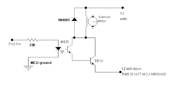
Solenoid and Sensor Control 4N35


To control the solenoid motors, we elected to use optoisolators. The control pins of the MCU were attached to the optoisolators which turns on and off the solenoid by controlling a TIP31 transistor. The TIP31 serves as an on/off switch for the solenoid. The optoisolators (4N35) were needed so that the MCU was completely isolated from the circuit. This protected the MCU because there were no physical connection between the MCU and the power supply. The 4N35 works by using a phototransistor that senses LEDS when the device is turned on.


The sensors were measured by a voltage division circuit coupled with an operational amplifier to achieve the desired results. The voltage outputted from the sensors was sent to the ADC of the MCU. The reference voltage of the MCU ADC was set to 5.0 volts which would correspond to the digital value 255 since only the top 8 bits of the ADC were used. We simply used this digital value to determine exactly how much juice we have dispensed.

3/19/2013

A Simple TX for Experimentation 2N7002 project


OK, so back to practical stuff on the bench. I breadboarded a simple push-pull power-oscillator using a pair of 2N7000 MOSFETs, operating in the HF region. (I've attached an LTSpice model if you want to tinker with it, I used a 2N7002 model and asymmetric bias resistors to keep spice happy, the real circuit uses 2N7000s and starts just fine with 4k7 bias resistors on both sides.)

The "180p" capacitor tunes the tapped coil to the frequency of operation, select or make it variable as desired. In one implementation I put 6v8 zener diodes on the MOSFET gates to protect them against over-voltage destruction, at low powers this is not strictly needed, but at higher powers you may need them. Similarly the pair of 33 pF feedback capacitors need to be selected with the frequency of operation in mind. The MOSFET drain breakdown voltage is also important if you are trying to scale up this circuit. While simple, other approaches are probably better for high powers, the MOSFETs are spending a lot of time in their transition regions, dissipating a lot of power. A purely switching class-E approach is obviously better, but suffers from sensitivity of tuning to load impedance in my brief experiments with it (using an IRF510 device). (I've attached another spice model attempting to show the class-E TX approach, I started with values derived using my class-E power amplifier design calculator, as shown it is not perfectly tuned. The practical circuit tunes up nicely and is quite efficient > 70%.) The breadboard TX in the video above is a class-C version with weak capacitive coupling to the tank to optimise its Q. Yet another approach is half or H-bridges, these show great promise, perhaps driving a magnetically coupled "link" winding rather than the tank directly, allowing the tank to float, and facilitating easy variation of coupling to it to optimise its Q... A subject for more detailed investigation at a later date perhaps.

3/17/2013

Circuit Power Amplifier OTL 50W by 2N3055


If you are seeking power Amplifier at loud good sound , durable and economize. I begs for to advise Circuit Power Amplifier OTL 50Watt by 2N3055 , because of use the equipment that seek good easy and build not difficult with. Many you who tell amp OTL the sound is not good. Me chest edge that be not the loud sound is excellent. Then like to use general ( in the past ) although in contain divide still have use. I like it fining decorates the circuit. Just you feed power supply 50V 2A also the work has already and a loudspeaker should use 8ohm 12 inc. sizes. Besides still model PCB for the convenience of friends. Request have fun Power Amplifier OTL 50Watt , please sir.

3/12/2013

Driving stepper motor using ULN2003


The simplest way to drive stepper motor having lower current rating is using ULN2003. The ULN2003 contains seven darlington transistors. The ULN2003 can pass upto 500mA per channel and has an internal voltage drop of about 1V when on. It also contains internal clamp diodes to dissipate voltage spikes when driving inductive loads. The circuit for driving stepper motor using ULN2003 is shown below.


For higher current torque motors, you can use TIP120. The advantage is that the TIP120 can pass more current along with heat sink. The disadvantages are that the more wiring is required and four TIP120 is used to control the motor.

3/07/2013

Microcontroller interface using RS485 & RS422


After a period of research, I found out that RS485 and RS422 is in fact the same.

RS422 is a duplex configuration. RS422 using 4 wire to communicate in both direction. One pair of wire to do transmit and the other pair to receive. Both sides is able to transmit and receive at the same time.

RS485 is a half duplex configuration. RS485 using only 2 wire to communicate in both direction. With only two wire, it means that when one side is transmitting, the other side of the communication line will be receiving. Both side cannot be transmitting at the same time. For RS485 transceiver, use MAX485 or MAX3485. They have the same pin out except that MAX485 uses 5V supply, MAX3485 uses 3.3V supply.

RS422 can be connected to work with RS485 to either receive or transmit date, but not both. RS422 can be wired directly using a pair of wire, +ve to +ve, -ve to -ve terminal. For RS422 transceiver, use MAX488 or MAX3488. They have the same pin out except that MAX488 uses 5V supply, MAX3488 uses 3.3V supply.

3/06/2013

AD620 Low Cost, Low Power Instrumentation Amplifier

The AD620 is a low cost, high accuracy instrumentation amplifier that requires only one external resistor to set gains of 1 to 1000. Furthermore, the AD620 features 8-lead SOIC and DIP packaging that is smaller than discrete designs, and offers lower power (only 1.3 mA max supply current), making it a good fit for battery powered, portable (or remote) applications.The AD620, with its high accuracy of 40 ppm maximum nonlinearity, low offset voltage of 50 mV max and offset drift of 0.6 mV/°C max, is ideal for use in precision data acquisition systems, such as weigh scales and transducer interfaces. Furthermore, the low noise, low input bias current, and low power of the AD620 make it well suited for medical applications such as ECG and noninvasive blood pressure monitors.The low input bias current of 1.0 nA max is made possible with the use of Superbeta processing in the input stage. The AD620 works well as a preamplifier due to its low input voltage noise of 9 nV/ÖHz at 1 kHz, 0.28 mV p-p in the 0.1 Hz to 10 Hz band, 0.1 pA/ÖHz input current noise. Also, the AD620 is well suited for multiplexed applications with its settling time of 15 ms to 0.01% and its cost is low enough to enable designs with one inamp per channel. 


The log circuit consists of an instrumentation amp and an Op amp together with a diode-connectedtransistor that produces a voltage proportional to the logarithm of the current A circuit consisting of avoltage reference, an instrumentation amp,and an op amp,togetherwith a diode-connected transistor,acts as a reference circuit. A thermometer IC,a fixed-gain instrumentation amp,and a divider circuitprovide the necessary temperature compensation and scaling for a transfer function

Vout51.985 log10 (Vin/1V)

Vref must be set to 1.000 V and, with Vin 5Vref, the gain adjust has to be set so that VO 50 V. Calirelbration low input voltage is done by changing buffer A4's offset voltage.

3/05/2013

FR107 1.0AMP. Fast Recovery Rectifiers

This is one package pinout of FR107 .


FR107 1.0AMP. Fast Recovery Rectifiers.
 

  • ● Fast switching for high efficiency
  • ● Low cost
  • ● Diffused junction
  • ● Low reverse leakage current
  • ● Low forward voltage drop
  • ● High current capability
  • ● The plastic material carries UL recognition 94V-0
 

  • ●Case: JEDEC DO-41 molded plastic
  • ●Polarity: Color band denotes cathode
  • ●Weight: 0.012 ounces , 0.34 grams
  • ●Mounting position: Any

3/03/2013

IRFP250N Power MOSFET


Fifth Generation HEXFETs from International Rectifier utilize advanced processing techniques to achieve extremely low on-resistance per silicon area. This benefit, combined with the fast switching speed and ruggedized device design that HEXFET Power MOSFETs are well known for, provides the designer with an extremely efficient and reliable device for use in a wide variety of applications.

The IRFP250N TO-247 package is preferred for commercial-industrial applications where higher power levels preclude the use of TO-220 devices. The TO-247 is similar but superior to the earlier TO-218 package because of its isolated mounting hole.

IRFP250N Features

• Advanced Process Technology
• Dynamic dv/dt Rating
•175°C Operating Temperature
•Fast Switching
• Fully Avalanche Rated
•Ease of Paralleling
•Simple Drive Requirements

2/28/2013

The inverter failure-tolerant control of single-phase sine wave is studied BTA16-600B


The failure-tolerant control purpose lies in directing against different trouble sources and symptoms, take the corresponding fault-tolerant processing measure, compensate for trouble, dispel or repair automatically, in order to guarantee the apparatus continues safe reliability service, or regard sacrificing characteristic losses as the cost, guarantee the apparatus finishes its basic function within stipulated time. If you want to adopt failure-tolerant control, have structure or redundancy functionally in the real-time analysis system at first. Find through analyzing, as to the inverter circuit of single-phase full-bridge, in fact the structural redundancy exists. Can regard the whole-bridge circuit as the superposing of two pieces of half bridge converter, if can be after the gas switching tube trouble of the power of a bridge arm of the inverter of the full-bridge, blockade this bridge arm, reconstruct the characteristic of certain holding circuit as the half bridge converter of the whole-bridge circuit, realize failure-tolerant control. Fig. 1 is the equivalent electrical circuit that the circuit reconstructs after full-bridge circuit topology with fault-tolerant capability and first, two bridge arm switch troubles.


In Fig. 1a, divides into two the electric capacity C1 as half bridge converter of the direct-flow Filtering capacitance in the whole-bridge circuit, C2, links the first bridge arm middle point A with two electric capacity middle points o with the bidirectional thyristor VTr1, the bidirectional thyristor VTr2 links the second bridge arm middle point B with point o, forms full-bridge circuit topology with fault-tolerant capability in this way.
Normal working hour, VTr1, VTr2 is the off state, the circuit equivalent is the normal full-bridge inverter circuit. After the trigger impulse takes place and lose the trouble in the power tube VM1, adopt the fault-tolerant control strategy to close the power tube VM3 of the same bridge arm, touch off VTr2 to turn on at the same time, VTr1 keeps off, the whole-bridge circuit is reconstructed as the half bridge converter, the circuit equivalent, in order to pursue 1b at this moment. After the trigger impulse takes place and lose the trouble in the power tube VM2, adopt the fault-tolerant control strategy to close the power tube VM4 of the same bridge arm, touch off VTr1 to turn on at the same time, VTr2 keeps off, the whole-bridge circuit is reconstructed as the half bridge converter, the circuit equivalent, in order to pursue 1c at this moment. The original control device should carry on corresponding adjustment according to the change of the control objective after the circuit is reconstructed, in order to guarantee the characteristic maintains at the acceptable range.
Sum up the fault-tolerant control strategy as follows, suppose VMi i =1,2,3,4The trigger impulse is lost. The whole fault-tolerant control process can be divided into the following several step: Judge the switch position of the trouble in fault detection and diagnostic circuitry; Blockade the trigger impulse of power switch on VMi and the same bridge arm in control unit, touch off the bidirectional thyristor which connects this bridge arm; The control unit changes the controller parameter, it is topological after make it adapt to reconstructing.
On the foundation of analyzing in the principle and artificial experiment, have designed and made a low-powered experimental provision. The experimental parameter is: Switching frequency fs =10 kHz; Export the filtering inductance L =1 mH; Filtering capacitance C of the output =20 F; Input the Filtering capacitance C1 =C2 =1 000 F; Direct-flow input voltage Uin =48 V. All power switches adopt the power MOSFET of the Model IRF650A, the output voltage adopts the voltage to isolate the man of great talent AD202 to measure after partial pressure. The output current measures and adopts the electric current transducer of Hall of Model CSB6-50A. The sense resistor of electric current of elementary straight flow side adopts 4 times 0. The resistance of 3 / 2 W is connected in parallel. Input the filtering resistance and is formed by two pieces of 1 000 F electric capacity, o some connect A, B bipunctate with VTr2 by VTr1. The bidirectional thyristor chooses BTA16-600B, drive and choose the bidirectional thyristor to drive special purpose chip MOC3 021. The main control chip of the circuit adopts the Model TMS302LF2407A DSP, is finished implementation of failure diagnosis and fault-tolerant tactics by it.
Experimental analogy VM1 is on the appointed phase place 90 degrees, 170 degrees, 270 degrees The trigger impulse takes place to lose the trouble, after the testing signal is judged by DSP trouble diagnostic element, carry out the fault-tolerant control procedure, blockades VM2 trigger impulse, touches off VTr1, it is 2 fold to change the given sine wave uref.